Electronics Injection Molding
Electronics injection molding for housings, connector bodies, and insulating parts, with requirements defined around PCB/metal fit, specified resin grades, and repeatable dimensions
- Assembly fit: mating features and latch/seal geometry reviewed as CTQ at quote stage
- Material grade: resin selection aligned to specified requirement (e.g., UL rating)
- Dimensional repeatability: DFM focuses on shrink/warp drivers and tooling strategy
- Verification: inspection approach defined upfront; reports available (dimensional / CMM / FAI)
- Secure upload. NDA available upon request.
Injection Molding for Electronics Assemblies
Electronic and electrical assemblies use molded plastic parts such as housings, covers, connector bodies, coil bobbins, switch components, and insulating spacers. These parts are typically defined by mating geometry, insulation function, and specified resin requirements, including flame-retardant grades.
Kemal supports electronics injection molding from DFM review and mold design through molding and basic assembly. Inspection documentation is available when required (dimensional report / CMM / FAI). Common resins include PC, PC/ABS, PA, PBT, PPS, and LCP.

Electronics Injection Molding Capabilities
Capability | Details |
|---|---|
Parts we support | Device housings & covers, connector/terminal housings, coil bobbins, switch components, insulating spacers, sensor/module enclosures |
Electronics-critical interfaces | PCB/metal mating features, latch/snap geometry, sealing grooves, insulation features; CTQ features defined during quote/DFM |
Thin-wall capability | Thin-wall housings and connector features supported; typical wall sections reviewed from ~0.5–0.8 mm, depending on resin, flow length, and gate strategy |
Minimum features (reviewed) | Small ribs, slots, shutoffs, venting-sensitive edges reviewed case-by-case for tooling feasibility and flash risk |
Dimensional capability | Typical ±0.05 mm for electronics parts; tighter CTQ features reviewed based on geometry, resin behavior, and tooling strategy |
Warp & shrink control | Gate location, rib layout, wall transitions, venting, and cooling balance planned to reduce distortion and improve assembly stability |
Insert / terminal readiness | Insert-ready tooling supported (terminal pins, threaded inserts, metal components as required); insert location and shutoff design reviewed during DFM |
Alignment / concentricity (as required) | Insert alignment and concentric features controlled through datum strategy and tooling design; targets confirmed per drawing/CTQ needs |
Press capacity | 50–1,300 tons (small precision components through medium-size electronics housings) |
Typical part size / weight | From small PCB-mounted parts (<1 g) to housings/covers up to several hundred grams (case-by-case by geometry and material) |
Tooling options | Single-cavity, multi-cavity, family molds; hot runner / cold runner; insert-ready tooling where required |
Flame-retardant options | UL 94 grades available by specified resin grade (e.g., V-0 / V-2); halogen-free options depend on grade and requirement |
ESD considerations | ESD considerations | ESD requirements supported through material selection and application-specific review; surface resistivity targets confirmed per use case |
Common materials | PC, PC/ABS, PA6/PA66, PBT, PPS, LCP (others by request) |
Materials × typical electronics use | PC/PC-ABS: housings/covers; PBT: connector housings/terminal blocks; PPS/LCP: high-temperature or fine-feature connectors; PA: functional brackets and interfaces (final grade per requirement) |
Sampling & production scope | Prototype builds, bridge quantities, and stable mass production for electronics assemblies |
CTQ & inspection outputs | Measurement method aligned to CTQ features; dimensional report available on request; CMM data / FAI available where required |
Secondary operations | Basic assembly support available where required (insert installation / simple sub-assembly) |
Typical Electronic Components We Mold

Device Housings & Covers
Compact housings, front panels, and covers for electronic assemblies. Designed around interface features and cosmetic surface requirements.
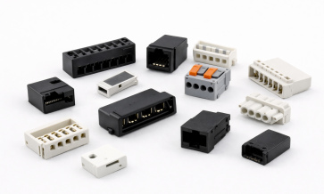
Connector & Terminal Housings
Molded connector bodies, terminal blocks, and plug/socket shells. Geometry supports stable mating and alignment at assembly.

Coil Bobbins
Bobbins for relays, transformers, and coil assemblies. Insulation features and geometry were kept stable for winding and fit.
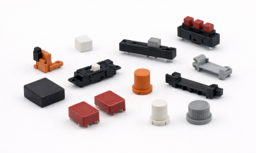
Switch Components
Switch caps, sliders, and functional interface parts. Built for repeatable tactile geometry and consistent assembly fit.

Insulating Spacers & Standoffs
Spacers, standoffs, and isolation parts for electronic layouts. Supports electrical isolation and controlled interface heights.
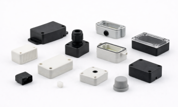
Sensor & Module Enclosures
Small enclosures and protective shells for sensors and modules. Interface and sealing features are supported where required.
Manufacturing Support for Electronics Assemblies

Custom Injection Mold Design
Mold design planned around PCB/metal interfaces, draft conditions, and gate locations that affect fit, warp, and assembly stability for electronics parts.
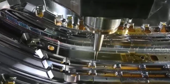
Tooling for Electronic Components
Tooling strategies are selected based on part geometry, material grade, and production volume, supporting stable molding of connectors, housings, and precision components.

Electronics Injection Molding
Plastic parts molded for electronics assemblies, with process control aligned to specified materials, dimensional requirements, and production consistency, from sampling through mass production.
Our Customers
Trusted by 500+ Global Innovators & Industry Leaders


FAQ's
What materials are commonly used for electronics injection molding (UL 94 V-0 options)?
Common materials used for electronics injection molding are selected based on flame-retardant performance, dimensional stability, electrical insulation, and long-term reliability. For projects requiring UL 94 V-0 ratings, the most commonly specified options include:
- PC (Polycarbonate): Widely used for electronic housings and covers. Offers good impact strength, dimensional stability, and is available in UL 94 V-0 grades.
- PC/ABS Blends: Common choice for consumer and industrial electronics enclosures. Balances toughness, heat resistance, and surface quality, with UL 94 V-0 and halogen-free grades available.
- PBT (Polybutylene Terephthalate): Frequently used for connector housings and terminal blocks. Provides good electrical insulation, chemical resistance, and stable dimensions, with UL 94 V-0 grades commonly specified.
- PA (Nylon 6 / Nylon 66, FR grades): Used for functional electronic components and brackets. Flame-retardant grades can meet UL 94 V-0, though moisture absorption is typically considered during design.
- PPS (Polyphenylene Sulfide): Applied in high-temperature electronics, power components, and precision connectors. Naturally flame-retardant and commonly meets UL 94 V-0 without additives.
- LCP (Liquid Crystal Polymer): Preferred for fine-pitch connectors and thin-wall electronic parts. Offers excellent flow, dimensional stability, and inherent flame resistance, typically UL 94 V-0.
Notes on UL 94 V-0 selection
UL ratings are resin-grade specific, not material-family generic
Halogen-free V-0 options are available depending on resin and supplier
Final material selection is typically confirmed during DFM and application review, considering wall thickness, part geometry, and end-use requirements
Can you mold connector housings and terminal blocks with tight pin alignment features?
Yes. Connector housings and terminal blocks with tight pin alignment features can be supported, provided the alignment requirements are defined at the drawing and DFM stage.
In electronics injection molding, pin alignment is typically controlled through a combination of tooling datum strategy, shutoff design, and insert/terminal positioning rather than relying on molding alone. During DFM review, mating interfaces, pin pitch, and critical alignment features are identified as CTQ features, and the tooling approach is planned accordingly.
Key points to be aware of:
Alignment capability is geometry- and resin-dependent
Final tolerances depend on part size, pin pitch, resin behavior (shrinkage), and tooling layout.Insert / terminal features are reviewed during DFM
Pin locations, retention features, and shutoffs are evaluated to minimize shift, flash risk, and cumulative tolerance stack-up.Verification can be provided when required
Dimensional inspection, CMM data, or FAI can be supplied for pin location and alignment features based on project requirements.
For projects with especially tight pin pitch or mating requirements, alignment targets are confirmed before tooling release, not after production starts.
How do you control warpage on electronic housings and covers?
Warpage on electronic housings and covers is controlled by addressing the main drivers—uneven shrinkage, unbalanced filling/packing, and non-uniform cooling—starting at DFM and carried through tooling and processing. In practice, we control it in four areas:
DFM and geometry corrections
Balance wall thickness and avoid abrupt transitions
Use ribs/gussets with appropriate thickness ratios to reduce sink and distortion
Review snap-fits, bosses, and large flat panels as CTQ warpage risk areas
Gate, runner, and venting strategy
Place gates to promote balanced fill and packing across large surfaces
Tune runner layout to reduce flow-length imbalance and differential shrink
Add venting at end-of-fill to prevent burn/short-pack that can create localized warp
Cooling and mold temperature control
Design cooling channels to equalize temperature across the cavity, especially around thick sections and bosses
Control mold temperature uniformity to reduce differential shrink across the part
Use inserts/baffles where needed to pull heat from hot spots
Process window and sampling controls
Establish a stable packing/hold profile to minimize shrink variation
Validate the process window during sampling and adjust to hit flatness/fit targets
Confirm warpage on defined datums/features and, when required, document results in inspection reports
If you share the housing CAD (STEP) and the surfaces that drive assembly (mating faces, latch features, sealing grooves), we can flag the highest warpage risks during DFM and propose specific gate/cooling and geometry adjustments.
Do you support insert molding for terminals, threaded inserts, or metal shields?
Yes. Insert molding for terminals, threaded inserts, and metal shields is supported, provided the insert requirements are defined during quoting and DFM.
How we approach insert molding for electronics:
DFM-first planning
Insert type, material, retention features, and critical datums are reviewed early. Mating interfaces and alignment features are identified as CTQ before tooling release.Tooling & shutoff design
Tooling is designed with dedicated shutoffs, locators, and datum references to control insert position, prevent flash, and reduce shift during molding.Insert placement control
Manual or semi-automated placement is selected based on volume and tolerance needs. Placement method is validated during sampling.Alignment & concentricity (as required)
Positional accuracy targets are confirmed per drawing. Insert alignment is controlled through tooling datum strategy rather than post-process correction.Verification options
Dimensional inspection, CMM data, or FAI can be provided for insert location and related features when required.
Final capability depends on insert geometry, resin selection, part design, and tolerance requirements, all of which are confirmed during DFM.
What tolerances can you hold for fit-critical PCB or metal interfaces?
For fit-critical PCB or metal interfaces, tolerances are defined and controlled as CTQ features during quoting and DFM rather than applied as a blanket value.
Typical guidance:
General molded features: ±0.05 mm is commonly achievable for electronics housings and interface geometry.
Fit-critical interfaces (PCB locating features, metal mating faces, latch/seal geometry): Tighter targets can be supported case-by-case, depending on part geometry, resin behavior, tooling strategy, and feature location.
How tolerance is controlled:
CTQ definition at DFM: Critical datums, mating features, and interface surfaces are identified upfront.
Tooling strategy: Gate placement, shutoff design, and datum references are planned to minimize variation at interface features.
Material behavior: Shrinkage and stability of the specified resin are considered when setting achievable targets.
Process window validation: Packing, cooling, and mold temperature are tuned during sampling to hold interface dimensions.
Verification: Dimensional inspection, CMM data, or FAI can be provided for fit-critical features when required.
If you share the CAD and indicate which PCB or metal interfaces drive assembly fit, we can confirm realistic tolerance targets before tooling release, not after production starts.
What inspection reports are available (FAI/CMM/dimensional reports/material certs)?
Inspection and documentation options are provided based on your drawing and acceptance requirements. Commonly available reports include:
Dimensional inspection reports
Measurement results for specified features and CTQ dimensions, typically taken from first articles or defined production samples.CMM measurement data
Coordinate Measuring Machine data for complex geometry, GD&T features, or tight-tolerance interfaces where higher measurement accuracy is required.FAI (First Article Inspection)
First Article Inspection reports prepared to your specification, commonly used for initial validation before production release.Material certificates
Resin material certifications or grade confirmations supplied by the material manufacturer, provided upon request.
Inspection methods and documentation scope are defined during quoting or DFM to align with CTQ features and program needs. Reports can be delivered for sampling, pilot builds, or ongoing production as specified.
Can you support injection molding services from prototype to bridge and mass production for electronics programs?
Yes. We can support electronics injection molding from prototype builds through bridge quantities and stable mass production, with tooling, process planning, and inspection aligned to your drawing requirements.
Prototype builds: validate fit-critical PCB/metal interfaces and confirm CTQ measurement methods.
Bridge quantities: support pilot demand while finalizing tooling and process window for repeatable output.
Mass production: run under a defined process window with inspection documentation and traceability applied as required.
To quote accurately, share your CAD (STEP/IGES), target resin/UL requirement, expected volumes across stages, and any CTQ or documentation needs (dimensional report / CMM / FAI / material certs).
What secondary operations do you support (heat staking / ultrasonic welding / basic assembly)?
Yes. Secondary operations are supported as required by the electronics assembly, with scope defined during quoting and DFM.
Common secondary operations include:
Heat staking: Used to secure metal pins, threaded inserts, or plastic bosses after molding. Stake locations and head geometry are reviewed to protect nearby cosmetic and functional features.
Ultrasonic welding: Applied for joining housings, covers, or multi-part enclosures. Joint design (energy directors, weld ribs) is reviewed during DFM to ensure consistent weld strength and alignment.
Basic assembly: Simple sub-assembly such as insert installation, part-to-part assembly, or hardware installation, where required for delivery or downstream integration.
Secondary operations are evaluated case-by-case, based on part geometry, material selection, tolerance requirements, and volume. The final scope and validation method are confirmed before production release.
When should you use overmolding instead of standard electronics injection molding?
Standard electronics injection molding is typically used for plastic housings, covers, connector bodies, bobbins, and other rigid components where the focus is on dimensional repeatability, insulation performance, and assembly fit. Overmolding is usually the better choice when the part also needs sealing, strain relief, or direct molding over cables, terminals, connectors, sensors, or PCB-related assemblies.
For example, if your project involves cable exits, connector backshells, sealed sensor interfaces, or integrated protection around electronic sub-assemblies, electronic overmolding is often more suitable than a standard molded housing because it combines protection and functional geometry into one molded structure. Learn more about our electronic overmolding solutions for connectors, cables, and PCB modules.
Explore More Industries We Support
Years of serving various clients gave us the experience and knowledge needed to support numerous industries. Click on the link below to know more.


